
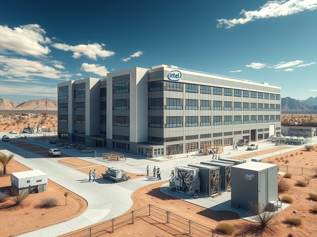

In the arid expanse of Phoenix Valley, Intel has invested more than $20 billion into a massive four-story semiconductor fabrication plant—Fab 52—which stands at the heart of the company’s bold turnaround plan. This facility is envisioned as Intel’s proof point: that it can once again lead in chip manufacturing rather than merely designing silicon.
Rebooting U.S. Chip Production
Inside Fab 52, Intel is deploying a next-generation manufacturing process that aims to deliver chips with greater performance and energy efficiency. For the first time in nearly a decade, Intel is using ASML’s lithography machinery in a U.S. plant to etch its most advanced semiconductors. During a recent tour, two of these cutting-edge machines—each costing in the range of $250 million—sat largely idle, as ASML engineers in cleanroom suits calibrated them. Nearby, two trailer-sized footprints awaited installation of future units, suggesting Intel expects to scale up capacity.
Intel has quietly invited prospective clients to visit Fab 52 in Chandler, Arizona, inviting them to consider offloading their chip production to Intel’s foundry. Yet many observers caution that chip designers will likely wait until Intel proves it can reliably manufacture its own designs before entrusting their arrays for smartphones, AI systems, or data center accelerators to Intel.
A Make-or-Break Moment
Fab 52 is more than just a factory: it is a litmus test. Once a symbol of Silicon Valley’s industrial might, Intel has fallen behind rivals in both design and process. The company’s inability to adopt ASML’s EUV tools in time let TSMC leapfrog it in foundry technology. As Intel’s chips lagged behind in battery life and performance, Apple and others shifted away from Intel.
Shrinking revenues precipitated a leadership carousel. In March, Intel named Lip-Bu Tan its third CEO in less than five years. He stepped into a fraught balance sheet and a risky strategy: to roll out five new process nodes over four years, while transitioning Intel into a full-fledged foundry for third-party chipmakers.
To shore up finances, Intel secured an $8.9 billion investment from the U.S. government in August, in exchange for a 10 % equity stake. That infusion was derived from funds authorized under the CHIPS and Science Act (2022), a federal initiative to revitalize U.S. semiconductor manufacturing.
Back in 2021, as Congress debated the CHIPS Act, Intel committed to building two new fabs—Fab 52 and Fab 62—on its Ocotillo campus in Arizona, pledging $32 billion of investment. The legislative backing made those plans more viable. Now, Tan’s challenge is to execute the second half: delivering a credible technological revival.
18A, Panther Lake, and the Stakes
At a recent event for industry analysts and media, Sachin Katti, Intel’s Chief Technology Officer, framed the situation bluntly: the 18A process and the upcoming Panther Lake chip architecture are “foundational to our future.” He added that Intel was making “two massive bets” and that their success was “mission-critical not just for Intel but for our country.”
Historically, Intel’s advantage lay in methodically staging technology transitions: debuting a new process node on a legacy chip, stabilizing yields, and then applying it to next-generation designs. But now, Intel is attempting to leap two dimensions at once—process and architecture concurrently.

The 18A node, using ASML’s extreme ultraviolet (EUV) tools, allows Intel to stack transistors vertically—a “3D stacking” approach that reduces footprint. It also flips the conventional paradigm: power is now delivered from the chip’s backside (instead of top) to avoid interference with data lines. The result is a denser, more efficient chip—Intel claims one can stack 10,000 sheets of silicon in a space thinner than paper.
Panther Lake, built on 18A, is intended to power AI workloads on laptops and support full-day computing. Intel projects shipments to begin late this year, with broader availability in early 2026. If the process works, Intel is shifting even its own production from external partners back to its internal fabs.
Analysts warn that combining risky new processes with novel architectures increases the chance of failure—especially when a single dust particle can ruin a wafer. As Ben Bajarin (Creative Strategies) put it: “The product has to be good, and the process has to be good.” Only when both succeed will the industry accept that “Intel can again fire on all cylinders.”
Yield Woes and a Cautious Road Ahead
Intel faces real challenges. Late last year, the company informed some clients that yield rates for its 18A process were lagging behind rivals. At the time, TSMC reportedly produced 30 % of its 2 nm chips without defects, while Intel’s defect-free yield was under 10 %. During the recent fab tour, Intel declined to disclose current yield metrics; analysts say those numbers likely won’t surface until next year’s financial reports.
If Intel can bring more chip production in house, it may reduce its dependency on foundries like TSMC and improve margins—if it can also attract external customers to fill Fab 52’s unused capacity. As Patrick Moorhead (Moor Insights) observes, Intel doesn’t currently have enough own‐workload to saturate Fab 52. The key is to secure major “anchor tenants” like Nvidia or Apple to give the foundry business real credibility.
In that sense, Fab 52 is akin to a shopping mall: without one or two marquee tenants, foot traffic (or wafer orders) may not reach viable levels. If Intel can land that anchor customer, as Moorhead says, “It would be game on.”


Emerging Signals & Strategic Shifts
Recent developments suggest Intel is pressing forward aggressively. The company now claims its new Panther Lake processor, fabricated at Fab 52, will deliver more than 50 % performance uplift over its prior generation, while offering 15 % better performance-per-watt and 30 % greater transistor density. These gains, if realized, would go a long way toward restoring Intel’s reputation as a process innovator. (Recent press also confirms that Panther Lake uses Cougar Cove P-cores and Darkmont E-cores. )
Yet risks remain. Some reports suggest Intel’s 18A node is encountering quality and yield hurdles—an outcome likened to a “Hail Mary” pass, where failure is not just possible but likely unless every element aligns.
Moreover, Intel has indicated it may delay or even cancel the next node, 14A, unless external customers commit. This would mark a more conservative shift: more tied investment and less speculative build-out.

Why the World Is Watching
Intel’s revival is not just a company matter—it has strategic significance. In an era of geopolitical tensions, advancing U.S. domestic semiconductor capability is a national priority. Fab 52 is more than a factory: it is a symbol of America’s ambition to rebuild its chip supply chain. Intel’s success—or failure—will send ripples across its relationships with OEMs, its leverage in government policy, and the future of chip sovereignty.
If Panther Lake proves stable and yields rise, it may finally persuade chip designers—many of whom today rely exclusively on TSMC—to consider Intel as a foundry partner. That shift could catalyze a new era of U.S.-based chip production and restore Intel’s standing. But if the yield remains weak or delays mount, critics will say Intel overreached.
In short, the stakes could not be higher. Fab 52 is Intel’s stake in the ground, and Panther Lake is its wager. The next year or two may decide whether Intel’s comeback is real—or another cautionary footnote in semiconductor history.




Leave a Reply